I2C TWI Tutorial From Rikipedia Embedded Wiki
Introduction
In modern electronic systems there are a number of peripheral ICs that have to communicate with each other and the outside world. To maximize hardware efficiency and simplify circuit design, Philips developed a simple bi-directional 2-wire, serial data (SDA) and serial clock (SCL) bus for inter-IC control. This I2C-bus supports any IC fabrication process and, with the extremely broad range of I2C-compatible chips from Philips and other suppliers, it has become the worldwide industry standard proprietary control bus. Each device is recognized by a unique address and can operate as either a receiver-only device (e.g. an LCD Driver) or a transmitter with the capability to both receive and send information (such as memory). Transmitters and/or receivers can operate in either master or slave mode, depending on whether the chip has to initiate a data transfer or is only addressed. I2C is a multi-master bus, i.e. it can be controlled by more than one IC connected to it.
The basic I2C-bus, with a data transfer rate up to 100 Kbits/s and 7-bit addressing, was originally introduced nearly 20 years ago. But, as data transfer rates and application functionality rapidly increased, the I2C-bus specification was enhanced to include Fast-mode and 10-bit addressing, meeting the demand for higher speeds and more address space. Most recently, High-speed Mode has been added; with speeds of up to 3.4 Mb/s it ensures the capacity of the I2C-bus to support existing and future high speed serial transfer rates for applications such as EEPROM and Flash memory.
I2C Bus Specification and Concept
The I2C-bus supports any IC fabrication process (NMOS, CMOS, bipolar). Two wires, serial data (SDA) and serial clock (SCL), carry information between the devices connected to the bus. Each device is recognized by a unique address (whether it's a microcontroller, LCD driver, memory or keyboard interface) and can operate as either a transmitter or receiver, depending on the function of the device. Obviously an LCD driver is only a receiver, whereas a memory can both receive and transmit data. In addition to transmitters and receivers, devices can also be considered as masters or slaves when performing data transfers (see Table 1). A master is the device which initiates a data transfer on the bus and generates the clock signals to permit that transfer. At that time, any device addressed is considered a slave.
| Term | Description |
|---|---|
| Transmitter | The device which sends the data to the bus. |
| Receiver | The device which receives the data from the bus. |
| Master | The device which initiates a transfer, generates clock signals and terminates a transfer. |
| Slave | The device addressed by a master. |
| Multi-Master | More than one master can attempt to control the bus. |
| Arbitration | Only one master can control the bus. |
| Synchronization | Procedure to sync. The clock signal. |
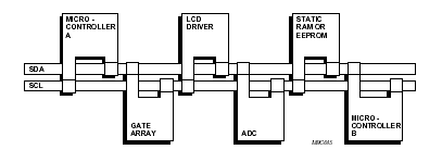
The I2C-bus is a multi-master bus. This means that more than one device capable of controlling the bus can be connected to it. As masters are usually micro-controllers, let's consider the case of a data transfer between two microcontrollers connected to the I2C-bus (see figure above).
- Suppose microcontroller A wants to send information to microcontroller B:
- Microcontroller A (master), addresses microcontroller B (slave).
- Microcontroller A (master-transmitter), sends data to microcontroller B (slave-receiver).
- Microcontroller A terminates the transfer.
- If microcontroller A wants to receive information from microcontroller B:
- Microcontroller A (master) addresses microcontroller B (slave).
- Microcontroller A (master-receiver) receives data from microcontroller B (slave-transmitter).
- Microcontroller A terminates the transfer.
Generation of clock signals on the I2C-bus is always the responsibility of master devices; each master generates its own clock signals when transferring data on the bus. Bus clock signals from a master can only be altered when they are stretched by a slow-slave device holding-down the clock line or by another master when arbitration occurs.
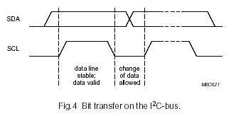
Data Validity Condition
The data on the SDA line must be stable during the HIGH period of the clock. The HIGH or LOW state of the data line can only change when the clock signal on the SCL line is LOW (see Fig.4).
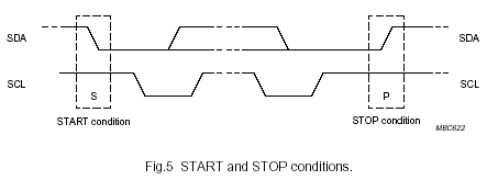
Start and Stop Condition
A HIGH to LOW transition on the SDA line while SCL is HIGH is one such unique case. This situation indicates a START condition.
A LOW to HIGH transition on the SDA line while SCL is HIGH defines a STOP condition.
START and STOP conditions are always generated by the master. The bus is considered to be busy after the START condition. The bus is considered to be free again a certain time after the STOP condition.
The bus stays busy if a repeated START (Sr) is generated instead of a STOP condition. In this respect, the START (S) and repeated START (Sr) conditions are functionally identical (see Fig.6). For the remainder of this document, therefore, the S symbol will be used as a generic term to represent both the START and repeated START conditions, unless Sr is particularly relevant.
Detection of START and STOP conditions by devices connected to the bus is easy if they incorporate the necessary interfacing hardware. However, microcontrollers with no such interface have to sample the SDA line at least twice per clock period to sense the transition.
Data Transfer
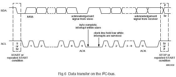
Byte Format:
Every byte put on the SDA line must be 8-bits long. The number of bytes that can be transmitted per transfer is unrestricted. Each byte has to be followed by an acknowledge bit. Data is transferred with the most significant bit (MSB) first (see Fig.6). If a slave can't receive or transmit another complete byte of data until it has performed some other function, for example servicing an internal interrupt, it can hold the clock line SCL LOW to force the master into a wait state. Data transfer then continues when the slave is ready for another byte of data and releases clock line SCL.
In some cases, it's permitted to use a different format from the I2C-bus format (for CBUS compatible devices for example). A message which starts with such an address can be terminated by generation of a STOP condition, even during the transmission of a byte. In this case, no acknowledge is generated.
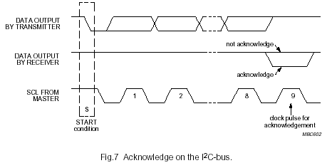
Acknowledge:
Data transfer with acknowledge is obligatory. The acknowledge-related clock pulse is generated by the master. The transmitter releases the SDA line (HIGH) during the acknowledge clock pulse.
The receiver must pull down the SDA line during the acknowledge clock pulse so that it remains stable LOW during the HIGH period of this clock pulse (see Fig.7). Of course, set-up and hold times must also be taken into account.
Usually, a receiver which has been addressed is obliged to generate an acknowledgement after each byte has been received. The master can then generate either a STOP condition to abort the transfer, or a repeated START condition to start a new transfer.
If a slave-receiver does acknowledge the slave address but, sometime later in the transfer cannot receive any more data bytes, the master must again abort the transfer. This is indicated by the slave generating the not-acknowledge on the first byte to follow. The slave leaves the data line HIGH and the master generates a STOP or a repeated START condition.
If a master-receiver is involved in a transfer, it must signal the end of data to the slave- transmitter by not generating an acknowledge bit on the last byte that was clocked out of the slave. The slave-transmitter must release the data line to allow the master to generate a STOP or repeated START condition.
Writing on I2C Bus
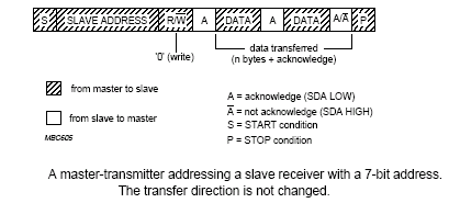
Figure above describes format of I2C frame when writing data to slave. In Frame above you see following terms:
| Term | Description |
|---|---|
| S | Start Condition |
| Sr | Repeated Start Condition |
| SLAVE ADDRESS | 7-bit Slave address |
| R/nW | Read/Write: Read - 1, Write - 0 |
| A | Acknowledge from slave |
| nA | Not Acknowledge |
| DATA | 8-bit Data |
| P | Stop Condition |
Shaded Area describes data transfer from Master controller to slave device, clear block describes data transfer from Slave to master controller.
Following is the sequence we need to follow when writing data:
- Send start condition.
- Send 7-bit slave address with read/write bit.
If we want to write on to slave device then R/W bit will be 0 and if a read is to be performed then R/W will be set to 1.
Example:
We want to write on an EEPROM memory with 7bit address as 0x50. We will append write bit to this 7-bit address.
[ (MSB) 7-bit address ] [r/w bit (LSB) ] = [ 8-bit address byte with R/W ]
0b10100000 -> 0xA0
- Slave will send Ack bit.
- Send data byte to slave and slave will acknowledge every byte, if its last byte to be sent, slave will reply with No-Acknowledge bit (NAK).
In case of EEPROM and certain devices which needs commands to be written into specific register addresses, first data byte is always the subaddress of that I2C device, which denotes the location where the following data is going to be written.
- Send stop condition to end data transfer.
We will get a better idea when we put this into action in coding.
Reading from I2C Bus
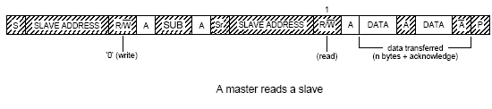
When reading from I2C bus, if you want to read from a specific location or (sub address) address usually in case of serial EEPROM or RTC etc., we need to send a dummy write byte to put the read pointer to that particular location. This dummy write is demonstrated in figure above. The data flow is explained below:
- Send start condition.
- Send 7-bit slave address with write bit (R/W = 0).
- Send sub address or location on I2C device where u want to read from, after this the internal address pointer of I2C device points to location where u want to read from.
This is called dummy write.
- Now send a repeated start condition.
- Send 7-bit slave address with read bit (R/W = 1).
- Now slave will send data to master and master will acknowledge after each byte read. If it’s the last byte to be read from slave then master will send a not acknowledge.
- Master send a stop condition to end the transfer.
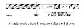
In case of reading a device with no sub addresses like ADC etc. then you just need to send slave address with read bit. As shown in figure below.
See Also
Learn to implement I2C on various microcontrollers like 8051, PIC and AVR. Visit the links below for further reading