Choosing of CT For the ADE7758


I am lined up with lot of queries, will get back shortly. Just preparing out the list

:bye
[ Edited Tue Jan 27 2009, 05:46 pm ]
hi sanath,
well, i have to confess i know as much as u do ( maybe even a little less now!pdi33
Now even I tooooo confess I do as much u guyz know
( hope I would have been lk this Ravana till I complete this project ) 
!dance

 ya ya sure PDI :-) I pray daily Lord Shiva to give me the source code of this project. might be he is also scratchng his head lk me :mad
 Ya now coming to Active, Reactive, & Apparent power ( looks lk sm 3D parameters
) 
If I am not wrong, the Active power is nothing but the actual power consumed and it is measured in terms of Killo-watt hours (KWh). and when the load contains reactive elements such as capacitance & inductance , because of that Current will be out of phase with the voltage by an angle. So as a result some kind of reactance is introduced into the line and the power associated with that is the Reactive power . and is measured in VAR Hours.:D and the Apparent power is the vector sum of active power & Reactive power & is measured in VA Hours. Practically I need to check out how this reactive power comes into picture, if there is no reactive elements in load then wat happens

then the next thing why I was not able to get the Active Power Pulsed o/p when I had given the Single phase to ADE. Since in ADE each phase is independent I think it has to work with single phase. The main reason is
The output from the DFC is divided down by a pair of frequency division registers before being sent to the APCF pulse output. Namely, APCFDEN/APCFNUM pulses are needed at the DFC output before the APCF pin outputs a pulse.
So until & unless I do the SPI Communication with ADE7758 for initializing the internal registers there is no other way I can check out the functionality. :-)
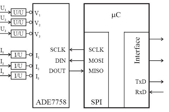
So now the problem is about the CPOL & CPHA settings in Master Controller.

So the ADE7758 tells Data is shifted into the ADE7758 at the DIN logic input on the falling edge of SCLK. Data is shifted out of the ADE7758 at the DOUT logic output on a rising edge of SCLK.
Wikipedia tells At CPOL=0 the base value of the clock is zero
* For CPHA=0, data is read on the clock's rising edge (low->high transition) and data is changed on a falling edge (high->low clock transition).
* For CPHA=1, data is read on the clock's falling edge and data is changed on a rising edge.
Can anyone have a better view on that :-)
:bye
Finally the writing of optimized Firmware code for SPI Communication with ADE chip been got over :-)
Even though I had started with Onchip SPI of P89V51RD2BN Controller, finally it got failed since the inbuilt Timing specifications for write and read operations won't match with slave since ADE has got 2 separate modes with communication register. and even we can't set the min delay required b/w the transfer of bytes.So had written the firmware code by taking up the four port pins based on the timing specifications given in datsheet :-)
So now I want to know is there any possibility of checking this firmware with the ADE chip without giving the specified inputs to the Current & voltage channel . Mean to say if suppose I write into ADE Register and after that If I read the same register whether I will be getting the value what has been written. or If I read the value of any register whether I will be getting the default value as mentioned in the data sheet.
Hi :-)
So now I want to know is there any possibility of checking this firmware with the ADE chip without giving the specified inputs to the Current & voltage channel . Mean to say if suppose I write into ADE Register and after that If I read the same register whether I will be getting the value what has been written. or If I read the value of any register whether I will be getting the default value as mentioned in the data sheet.SANATH EMBEDDED
Though they have specified that the Watt-hur accumulation registers are read-only, nothing seems to indicate the same to be true with the current /voltage channel RMS registers. So why don't u try it and practically check the results. The worst case would be u will get junk value after reading so no harm done. :-)


to do setup of CPHA and CPOL, its good to see timing diagrams instead of relying on written text. it always confuses you.
I suggest try with software SPI.
As far as i know there is some problem with P89V51RD2's SPI module, it seem not working as per expectations. Even shyam told me this. so be careful with itAjay
Vooooo my GOD :mad :mad :mad watz happening with this ADE7758 SPI Communication with RD2. Never expected this kind of strange problems :-s :-s :mad
When I was testing the simple SPI code ( making use of Onchip ) & even bit- banged approach code for simple serial write & serial read, so everytime I was getting the 0xFF or some other junk values. So to come out this problem I had started doing all the dramas
with CPOL & CPHA Settings and clk frequency settings. But one point after sm time when I pressed the Controller RESET , immediately I got the exact value what has been written into the register. So started analyzing this problem deeper & deeper after power on If I press the controller Reset after 45 secs the communication gets established with ADE7758. Even to be more precise after the power on If i put the huge delay of 45 secs , & after that If I write & read in to register, i will get the exact values. Even too check out that I put the these function in while loop and after around 45 secs I will get the exact o/p, otherwise everytime it will 0xFF. After that delay all the read & write operations works fine
without any delay.
while(1)
  {
        Write8_7758(0x13,0x03);
	delay_ms(1000);		  // Delay- 1000 millisecs
	P0 = Read8_7758(0x13);
}
Can anyone tell me Is this problem from the ADE7758 Slave or P89v51RD2BN
:mad
[ Edited Fri Feb 06 2009, 07:07 pm ]
to do setup of CPHA and CPOL, its good to see timing diagrams instead of relying on written text. it always confuses you.
I suggest try with software SPI.Ajay
Even today I have written the optimized Code for SPI Communication for ADE7758 with Bit- Banged approach for P89v51RD2BN by making use of 4 port pins of a controller in which also communication gets established after the 30 secs of Power ON
So I don't find any problem with onchip SPI of P89V51RD2BN controller
Even I checked out with other RPS power supply but in all the cases problem remains same. :-s
Is there anything problem with the SPI Bus. or without the i/p to channels of ADE7758 there may have indirectly high impedance on the SPI bus
:mad :mad :mad


